PY32F003L24D6TR DevLab Development Board
Introduction
The DevLab Development Board based on the PY32F003L24D6TR microcontroller is designed for rapid prototyping, embedded systems education, IoT experimentation, and wearable devices. This board combines flexible power options, modern connectivity, and accessible interfaces to accelerate your hardware development. The microcontroller features a 32-bit ARM Cortex-M0 core, up to 24 MHz clock speed, 16KB Flash memory, and 2KB SRAM, making it suitable for a wide range of applications. With built-in peripherals like SPI, I2C, UART, and a 12-bit ADC, the board supports diverse project requirements.
PY32f003L24D6TR Devlab
📦 Overview
| Feature | Description |
|---|---|
| Microcontroller | PY32F003L24D6TR (32-bit ARM Cortex-M0) |
| Memory | 24KB Flash, 4KB SRAM |
| Flash (Kbytes) | 16 |
| SRAM (Kbytes) | 2 |
| Advanced Timers (16-bit) | 1 |
| General Purpose Timers | 4 |
| Low Power Timer | 1 |
| SysTick | 1 |
| Watchdog | 2 |
| SPI | 1 |
| I2C | 1 |
| USART | 1 |
| DMA Channels | 3 |
| RTC | Yes |
| GPIOs | 7 |
| 12-bit ADC (ext+int) | 4+2 |
| Comparators | 2 |
| Max. CPU Frequency (MHz) | 24 |
| Operating Voltage (V) | 1.7 ~ 5.5 |
🧪 Use Cases
- Device Prototyping
- Embedded Systems Education
- Networked Alambric Devices
- Wearable Technology Development
📚 Resources
- Pinout Diagram
- Schematic Diagram
- Code Examples
- Datasheet components and peripherals
- Product Wiki
- Purchase Link
📝 License
All hardware and documentation in this project are licensed under the MIT License.
Please refer to LICENSE.md for full terms.
Hardware Overview
Technical Specifications
- Microcontroller: [Insert name and variant]
- Core Architecture: [Xtensa / ARM Cortex-M / RISC-V]
- Clock Speed: [e.g., 240 MHz]
- Flash / RAM: [e.g., 8 MB Flash, 2 MB PSRAM]
- Wireless: [2.4 GHz Wi-Fi, BLE 5.0]
- Interfaces: I2C, SPI, UART, ADC
- Connector: QWIIC + Pin Headers
- Power:
- Input via USB-C: 5V
- Regulated Output: 3.3V
- Battery Support: [Yes / No]
- Dimensions: [e.g., 55mm x 25mm]
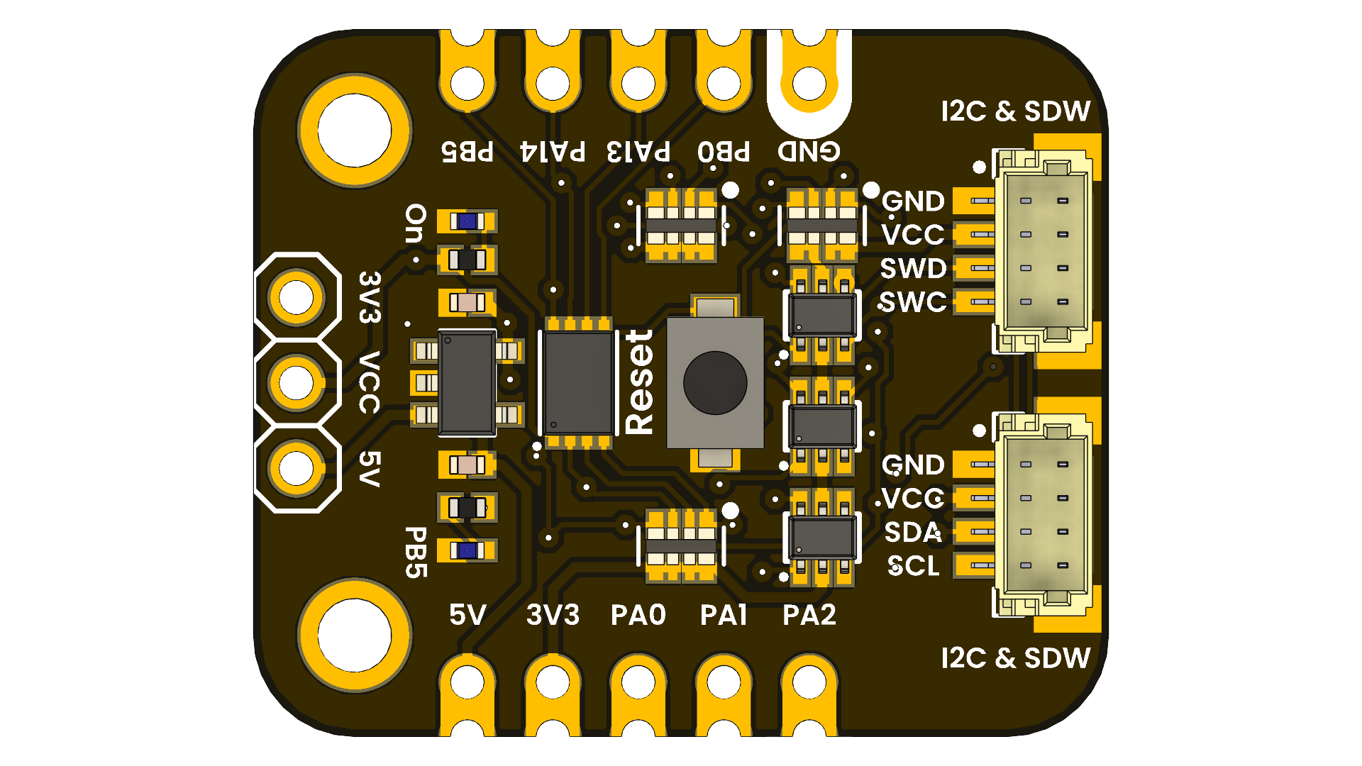
🔌 Pinout
Pinout Details
| Pin Label | Function / Notes |
|---|---|
| VCC | Power Input |
| GND | Ground |
| PA0 | USART2_TX MISO |
| PA1 | USART2_RX SCK |
| PA2 | ADC_IN2 CS |
| PB0 / PF2 | GPIO / NRST |
| PB5 | LED Built In / GPIO / MOSI |
| PA13 / PB6 | SWDIO / I2C_SCL |
| PA14 / PA10 | SWCLK / I2C_SDA |
Connectivity Options
- I2C: JST 1mm QWIIC connector (Power + I2C lines)
- SPI: JST 1mm connector (Power + SPI lines)
- GPIO: 2x 4-pin headers for general-purpose I/O
- SWD: Dedicated pins for programming and debugging
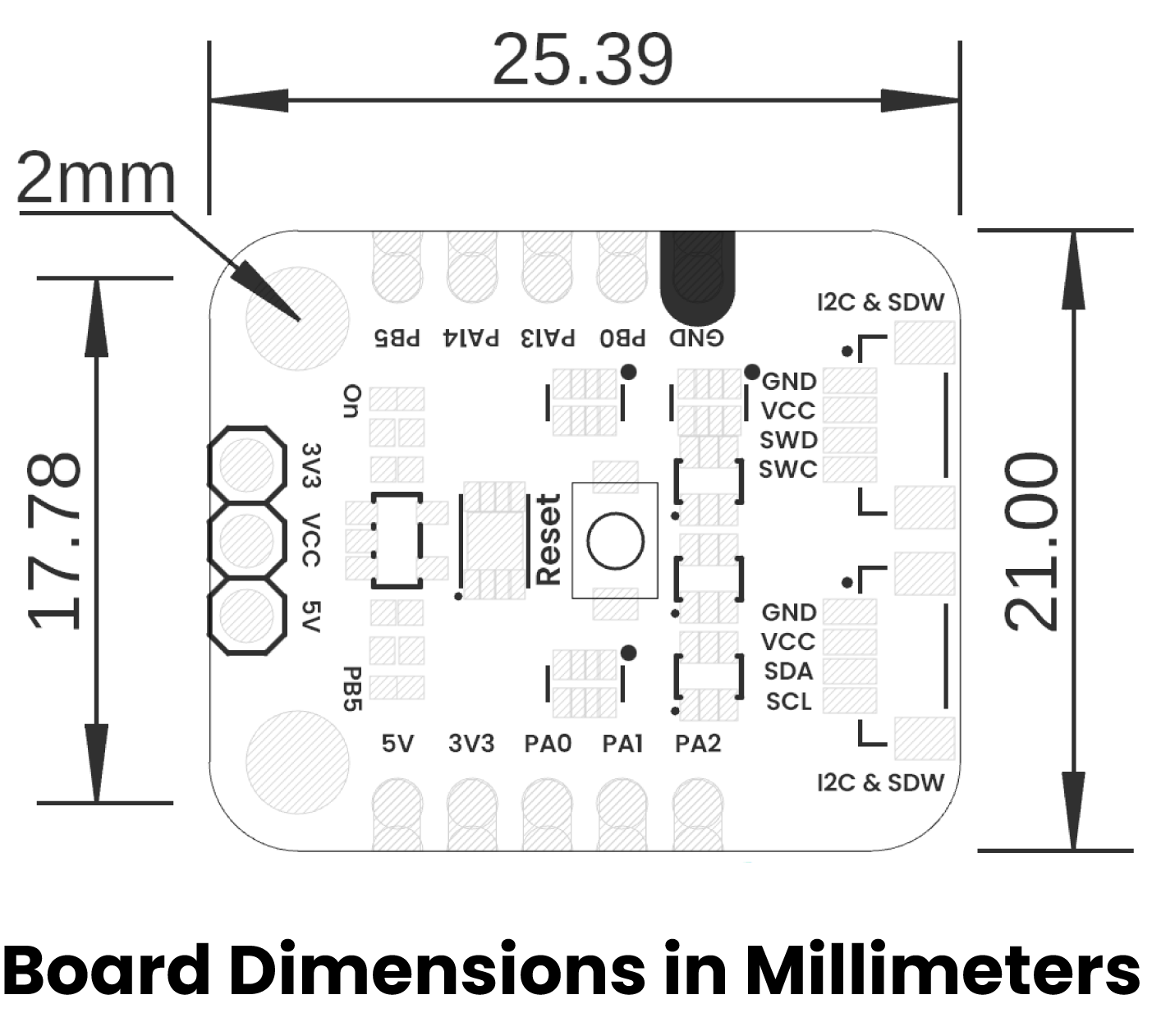
📏 Board Dimensions
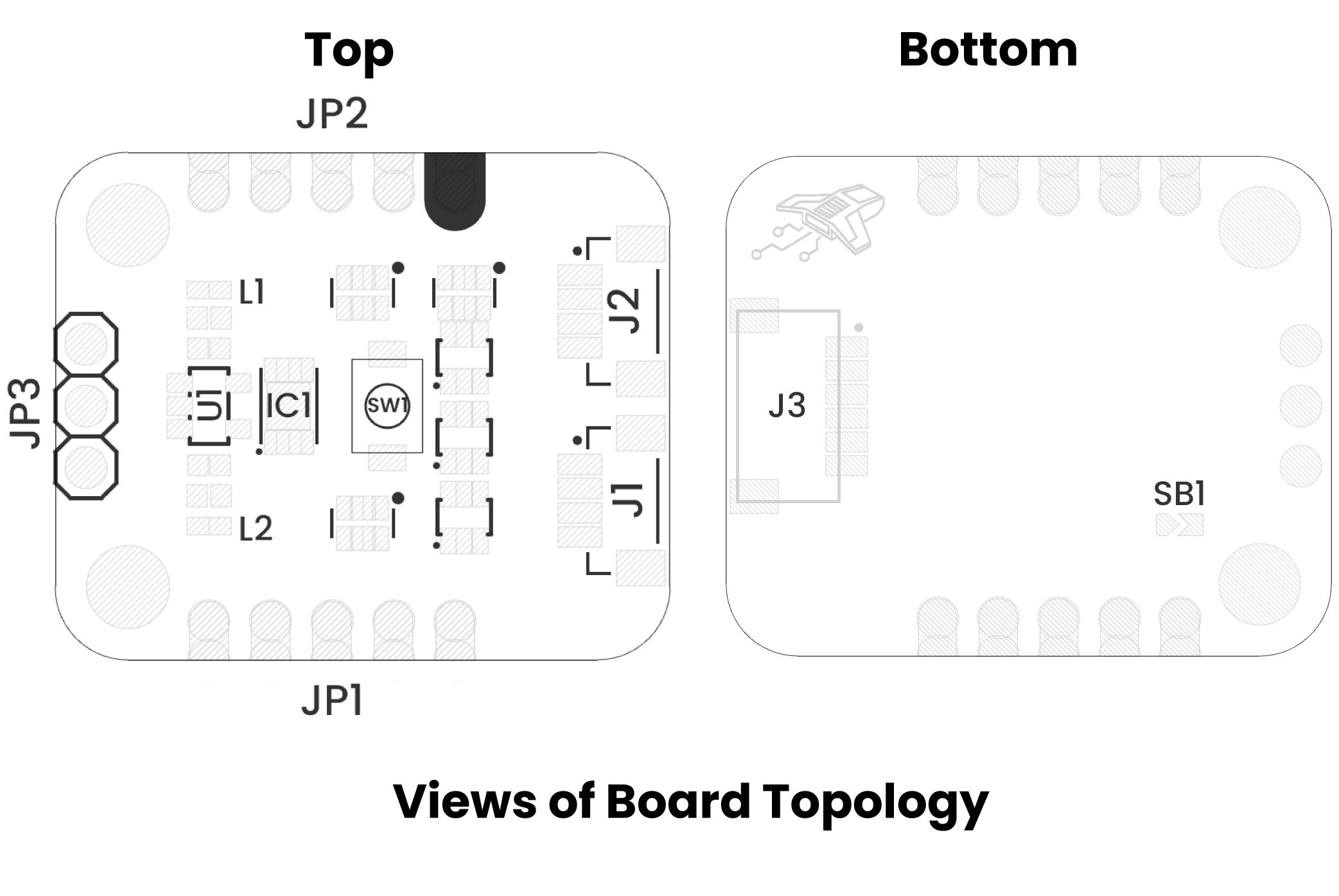
📃 Board Topology
| Ref. | Description |
|---|---|
| IC1 | PY32f003L24D6TR Microcontroller |
| U1 | AP2112K 3.3V Regulator |
| SW1 | Reset Push Button |
| L1 | Power On LED |
| L2 | Built In LED to PB5 |
| J1 | JST 1mm Connector for I2C or JTAG |
| J2 | JST 1mm Connector for I2C or JTAG |
| J3 | JST 1mm Connector for SPI |
| JP1 | Header for GPIOs |
| JP2 | Header for GPIOs |
| JP3 | Header for Power Supply Selection |
| SB1 | Solder Bridge to Enable LED Built In |
References
Technical Specifications
- Microcontroller: [Insert name and variant]
- Core Architecture: [Xtensa / ARM Cortex-M / RISC-V]
- Clock Speed: [e.g., 240 MHz]
- Flash / RAM: [e.g., 8 MB Flash, 2 MB PSRAM]
- Wireless: [2.4 GHz Wi-Fi, BLE 5.0]
- Interfaces: I2C, SPI, UART, ADC
- Connector: QWIIC + Pin Headers
- Power:
- Input via USB-C: 5V
- Regulated Output: 3.3V
- Battery Support: [Yes / No]
- Dimensions: [e.g., 55mm x 25mm]
Pinout
Pinout Details
| Pin Label | Function / Notes |
|---|---|
| VCC | Power Input |
| GND | Ground |
| PA0 | USART2_TX MISO |
| PA1 | USART2_RX SCK |
| PA2 | ADC_IN2 CS |
| PB0 / PF2 | GPIO / NRST |
| PB5 | LED Built In / GPIO / MOSI |
| PA13 / PB6 | SWDIO / I2C_SCL |
| PA14 / PA10 | SWCLK / I2C_SDA |
Connectivity Options
- I2C: JST 1mm QWIIC connector (Power + I2C lines)
- SPI: JST 1mm connector (Power + SPI lines)
- GPIO: 2x 4-pin headers for general-purpose I/O
- SWD: Dedicated pins for programming and debugging
Board Dimensions
Board Topology
| Ref. | Description |
|---|---|
| IC1 | PY32f003L24D6TR Microcontroller |
| U1 | AP2112K 3.3V Regulator |
| SW1 | Reset Push Button |
| L1 | Power On LED |
| L2 | Built In LED to PB5 |
| J1 | JST 1mm Connector for I2C or JTAG |
| J2 | JST 1mm Connector for I2C or JTAG |
| J3 | JST 1mm Connector for SPI |
| JP1 | Header for GPIOs |
| JP2 | Header for GPIOs |
| JP3 | Header for Power Supply Selection |
| SB1 | Solder Bridge to Enable LED Built In |
References
Getting Started
Quick Setup
1. Hardware Connections
| Pin | Description | Notes |
|---|---|---|
| VCC | 3.3V or 5V supply | Power supply |
| GND | Ground | Common ground |
| SDA | I2C Data Line (SDA) | Connect to microcontroller I2C SDA pin |
| SCL | I2C Clock Line (SCL) | Connect to microcontroller I2C SCL pin |
| D0 | Digital I/O (separate connection) | Not included in QWIIC connector, must be connected separately |
Note: Compatible with JST 1 mm pitch QWIIC connector for easy I2C integration (power only, D0 must be connected separately).
2. Software Installation
| Feature / Peripheral | PY32F003L24D6TR |
|---|---|
| Flash (Kbytes) | 16 |
| SRAM (Kbytes) | 2 |
| Advanced Timers (16-bit) | 1 |
| General Purpose Timers | 4 |
| Low Power Timer | 1 |
| SysTick | 1 |
| Watchdog | 2 |
| SPI | 1 |
| I2C | 1 |
| USART | 1 |
| DMA Channels | 3 |
| RTC | Yes |
| GPIOs | 7 |
| 12-bit ADC (ext+int) | 4+2 |
| Comparators | 2 |
| Max. CPU Frequency (MHz) | 24 |
| Operating Voltage (V) | 1.7 ~ 5.5 |
Package-Specific Information
            DFN8 Pinout (Top View):
               VCC  1 ┌─────┐ 8  PB5/LED
               PA0  2 │     │ 7  PA14-SWDCK/PB6
               PA1  3 │     │ 6  PA13-SWDIO/PA10
               PA2  4 └─────┘ 5  PB0/PF2-NRST
Pinout PY32F003L24D6TR DevLab Development Board
- VCC: Power input for the board
- GND: Ground connection
- PA0: USART2 transmit (TX) or SPI MISO function
- PA1: USART2 receive (RX) or SPI SCK function
- PA2: Analog input channel 2 (ADC_IN2) or SPI chip select (CS)
- PB0 / PF2: General-purpose I/O (GPIO) or external reset (NRST)
- PB5: On-board LED, general-purpose I/O (GPIO), or SPI MOSI function
- PA13 / PB6: Serial Wire Debug I/O (SWDIO) or I2C clock line (I2C_SCL)
- PA14 / PA10: Serial Wire Debug clock (SWCLK) or I2C data line (I2C_SDA)
Examples
Arduino/C++ Examples
The following examples demonstrate various features of this development board.
Datasheet & Documentation
📄 Professional Datasheet
Complete technical specifications and professional documentation.
📎 View Professional Datasheet - Interactive HTML version
📎 Download PDF Datasheet - Downloadable PDF version
🔗 Additional Resources
Hardware Resources
- 🔌 Schematic Diagram - Not found (looking for unit_sch_*.pdf)
- 📐 Board Dimensions - Physical specifications
- 🔧 Pinout Reference - Pin configuration details
Software Resources
- 💻 Getting Started Guide - Setup and first steps
- 📝 Code Examples - Arduino sketches and demos
- 🛠️ Development Setup - IDE configuration
External Links
- 🔗 Source Code Repository - Complete project files
📋 Quick Reference
| Resource Type | Description | Link |
|---|---|---|
| 📄 Datasheet (HTML) | Interactive technical specs | View |
| 📄 Datasheet (PDF) | Downloadable technical specs | |
| 🔌 Schematic | Circuit diagram | Not found |
| 📐 Dimensions | Board measurements | View |
| 🔧 Pinout | Pin configuration | View |
| 💻 Examples | Code samples | View |
| 🔧 Setup Guide | Getting started | View |
For the most up-to-date information, please refer to the official documentation and repository.
License
MIT License
Copyright (c) 2025 UNIT-Electronics-MX
Permission is hereby granted, free of charge, to any person obtaining a copy of this software and associated documentation files (the "Software"), to deal in the Software without restriction, including without limitation the rights to use, copy, modify, merge, publish, distribute, sublicense, and/or sell copies of the Software, and to permit persons to whom the Software is furnished to do so, subject to the following conditions:
The above copyright notice and this permission notice shall be included in all copies or substantial portions of the Software.
THE SOFTWARE IS PROVIDED "AS IS", WITHOUT WARRANTY OF ANY KIND, EXPRESS OR IMPLIED, INCLUDING BUT NOT LIMITED TO THE WARRANTIES OF MERCHANTABILITY, FITNESS FOR A PARTICULAR PURPOSE AND NONINFRINGEMENT. IN NO EVENT SHALL THE AUTHORS OR COPYRIGHT HOLDERS BE LIABLE FOR ANY CLAIM, DAMAGES OR OTHER LIABILITY, WHETHER IN AN ACTION OF CONTRACT, TORT OR OTHERWISE, ARISING FROM, OUT OF OR IN CONNECTION WITH THE SOFTWARE OR THE USE OR OTHER DEALINGS IN THE SOFTWARE.
This project is licensed under the MIT License - see the LICENSE file for details.