General Information#
The Multi-Protocol Programmer is a compact and versatile development tool designed for high-precision embedded system applications. It supports a broad range of protocols and device architectures, including AVR, ARM (CMSIS-DAP), and CPLD (MAX II). Its USB connectivity enables direct interfacing with standard development environments, enabling:
In-system programming (ISP)
Step-through debugging
Boundary-scan testing (JTAG)
Flash memory operations
Supported Architectures#
AVR — via ISP (SPI configuration)
ARM Cortex-M — via CMSIS-DAP and SWD
RP2040
PY32
STM32
CPLD/FPGA (MAX II) — via JTAG
All protocols are exposed via labeled headers or JST connectors, allowing fast, solderless prototyping.
This device connects to a host system via USB and allows the user to program and debug various microcontrollers and programmable logic devices.
Supported Interfaces#
JTAG, for full-chip debugging and boundary scan
SWD, for ARM Cortex-M series
SPI, for flash and peripheral programming
UART, for serial bootloaders and communication
GPIO, for bit-banging or peripheral testing
Interface |
Description |
Signals / Pins |
Typical Use |
|---|---|---|---|
JTAG |
Standard boundary-scan and debug interface |
TCK, TMS, TDI, TDO, nTRST |
Full chip programming, in-circuit test, debug |
SPI |
High-speed serial peripheral interface |
MOSI, MISO, SCK, CS |
Flash memory programming, peripheral data exchange |
SWD |
ARM’s two-wire serial debug and programming interface |
SWCLK, SWDIO |
Cortex-M programming and step-through debugging |
JST Header |
Compact connector for power and single-wire debug signals |
SWC (SWCLK), SWD (SWDIO), VCC, GND |
Quick-connect to target board for SWD and power |
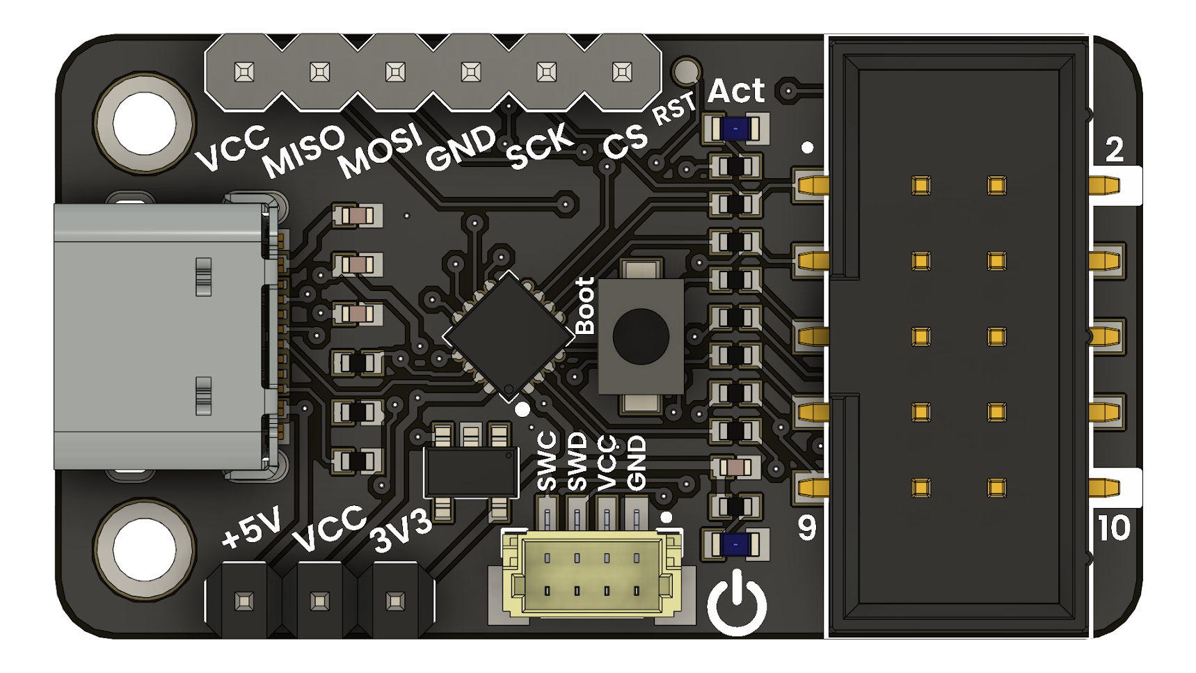
Sections GPIO Pin Distribution#
The Multi-Protocol Programmer features a set of GPIO pins that can be configured for various protocols, including JTAG, SWD, and ISP. These GPIOs are mapped to specific functions in the firmware, allowing users to adapt the programmer for different applications.
The GPIO pin distribution is defined within the CH552 firmware, supporting flexible assignment for various protocols. The firmware configures the specific mapping of GPIOs to protocols, such as SPI, JTAG, or SWD, based on the loaded configuration. Users can alter the pin distribution by modifying the firmware source code to suit their application requirements.
Protocol ISP – In-System Programming#
Compatible with AVR microcontrollers, this protocol allows programming and debugging via the SPI interface. The programmer can be used to flash firmware directly into the target device’s memory.
Fig. 1 Pinout diagram for CH552 Programmer#
PIN |
GPIO |
I/O |
|---|---|---|
MOSI |
1.5 |
MOSI, PWM1 |
MISO |
1.6 |
MISO, RXD1 |
CS |
3.3 |
PWM1, TXD0 |
SCK |
1.7 |
SCK, TXD1 |
Protocol JTAG#
Compatible with CPLD and FPGA devices, this protocol allows programming and debugging via the JTAG interface. The programmer can be used to flash firmware directly into the target device’s memory.
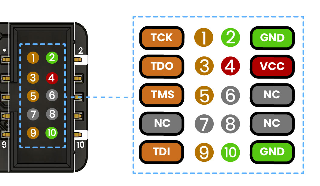
Fig. 2 Pinout diagram for CH552 Programmer#
PIN |
GPIO |
I/O |
|---|---|---|
TCK |
1.7 |
SCK, TXD1 |
TMS |
3.2 |
TXD1, INT0, VBUS1, AIN3 |
TDI |
1.5 |
MOSI, PWM1, TIN3, UCC2, AIN2 |
TDO |
1.6 |
MISO, RXD1, TIN4 |
PIN |
GPIO |
I/O |
|---|---|---|
NC 6 |
3.4 |
PWM2, RXD1, T0 |
NC 7 |
3.3 |
INT1 |
NC 8 |
1.4 |
T2, CAP1, SCS, TIN2, UCC1, AIN1 |
Protocol SWD#
Compatible with ARM Cortex-M microcontrollers, this protocol allows programming and debugging via the SWD interface. The programmer can be used to flash firmware directly into the target device’s memory.
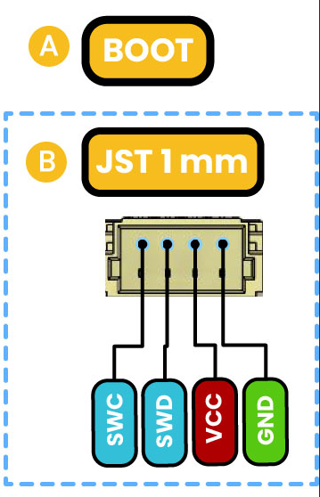
Fig. 3 SWD Pinout#
PIN |
GPIO |
I/O |
|---|---|---|
SWCLK |
1.7 |
SCK, TXD1, TIN5 |
SWDIO |
1.6 |
MISO, RXD1, TIN4 |
Note
GPIO numbers refer to the CH552 internal ports. Ensure correct firmware pin mapping before connecting external devices.
Fig. 4 Pinout diagram for CH552 Programmer#
Ref. |
Description |
|---|---|
IC1 |
CH552 Microcontroller |
U1 |
AP2112K 3.3V LDO Voltage Regulator |
PB1 |
Boot Push Button |
TP1 |
Reset Test Point |
TP2 |
P3.1 Test Point |
L1 |
Built-In LED |
L2 |
Power On LED |
SB1 |
Solder bridge to enable VCC at JTAG |
SB2 |
Solder bridge to enable VCC at JST |
J1 |
USB Type-C Connector |
J2 |
Low-power I2C JST Connector |
J3 |
JTAG Connector |
JP1 |
Header for SWD or ICSP programming |
JP2 |
Header to Select Operating Voltage Level |
Schematic Diagram